
- English
- 简体中文
- Español
- Português
- русский
- Français
- 日本語
- Deutsch
- tiếng Việt
- Italiano
- Nederlands
- ภาษาไทย
- Polski
- 한국어
- Svenska
- magyar
- Malay
- বাংলা ভাষার
- Dansk
- Suomi
- हिन्दी
- Pilipino
- Türkçe
- Gaeilge
- العربية
- Indonesia
- Norsk
- تمل
- český
- ελληνικά
- український
- Javanese
- فارسی
- தமிழ்
- తెలుగు
- नेपाली
- Burmese
- български
- ລາວ
- Latine
- Қазақша
- Euskal
- Azərbaycan
- Slovenský jazyk
- Македонски
- Lietuvos
- Eesti Keel
- Română
- Slovenski
- मराठी
- Srpski језик

Products


 Crystal")


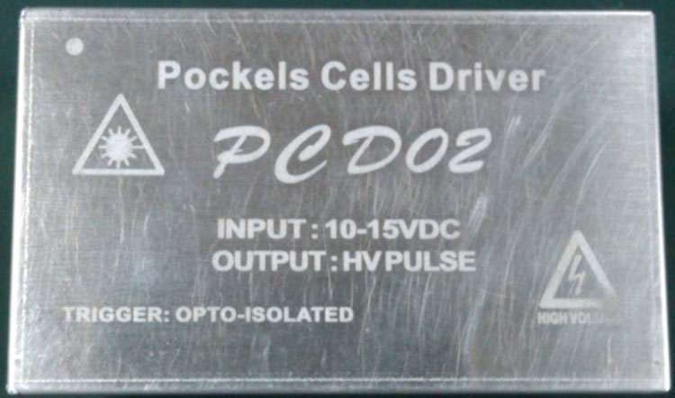
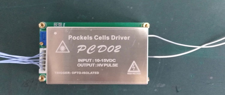
Q-Switch Pockels Cell Driver
We have many years of experience in the production of Q-Switch Pockels Cell Driver. Coupletech provides Pockels Cell driver PCD02 with compact design for Q-switches and Pockels Cell Modulator application, and it has mini size with 60*35*16mm. The input signal is +10-15VDC, and its output voltage is from 1000 to 4200V. The rising time and falling time is 10 ns, Output pulse width is 5 us, the repetition rate is from 0 to 2KHz.
Send Inquiry
Product Description
Q-Switch Pockels Cell Driver
|
APPLICATION Generation of high voltage pulses for the control of electro-optical Q-switches (Pockels cells) in a solid-state laser. Fast HV (less than 10 ns) edge ensures excellent pre-and post-pulse contrast. |
 |
Features
●Fast HV rise/fall time:<10 ns
●HV pulse amplitude:up to4.0 kV
●Pulse repetition rate: up to1000Hz
●Jitter, System Input to Output:<1.8ns
● TTL (CMOS) input signal required (3.3/5V, opto-isolated)
● Built-inHigh-Voltage source
● HV Voltage Control: “HV PROGRAM” potentiometer OR analog input.
SPECIFICATIONS
|
HVpulse amplitude |
1.0~4.0 |
kV |
|
|
Rise /Falltime |
≤10 |
ns |
Loadcapacitance:10PF |
|
HV pulse jitter |
≤1.8 |
ns |
|
|
Recovery time |
≤50 |
µs |
|
|
Voltage supply |
12 |
VDC |
12±0.5 V, <150 mA |
|
HV pulse repetition rate |
0~1000 |
Hz |
|
|
External triggering pulse amplitude requirement |
3.3–5 V |
V |
opto-isolated |
|
HV pulse delay |
70~90 |
ns |
|
|
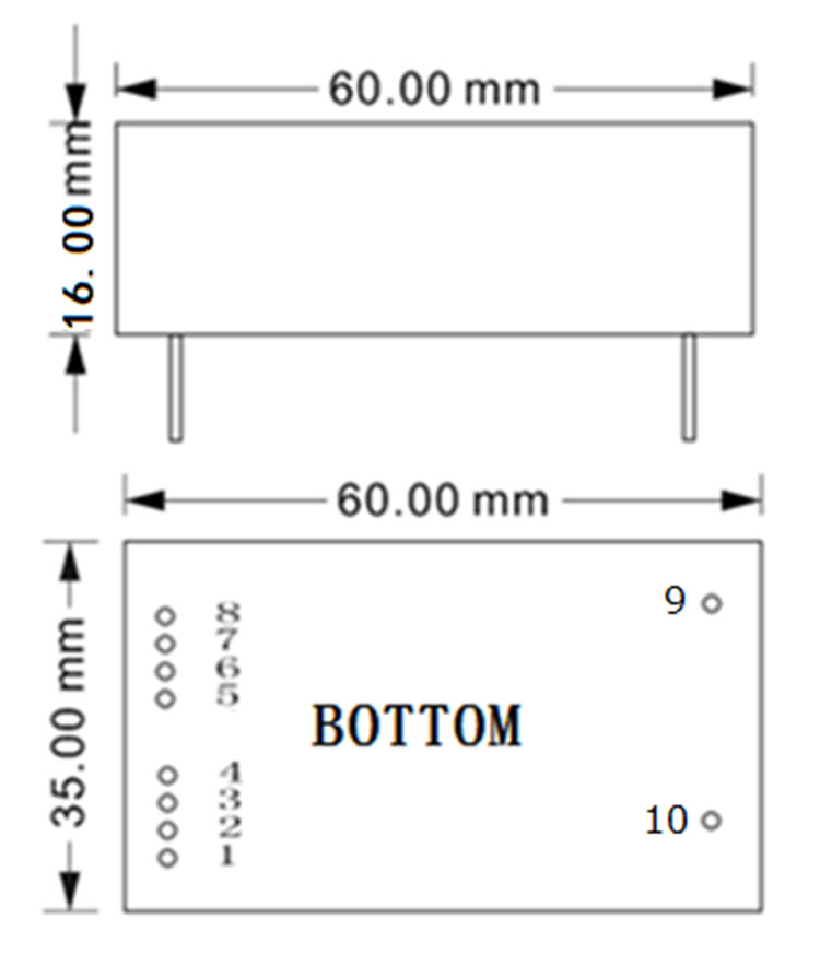
Dimensions |
60*35*16 |
mm |
|
|
Operating temperature |
-30~60 |
℃ |
|
Outline drawing of PCD02
|
PIN |
DESIGNATION |
DESCRIPTION |
|
1 |
SG- |
Step from “0” or ”1” on PIN11 PIN12 forms QSwitched pulse on Pockels Cell |
|
2 |
SG+ |
|
|
3 |
GND |
Return from power supply |
|
4 |
+12V |
Input Power Supply |
|
5 |
FB |
HV Voltage Control: “HV PROGRAM” potentiometer OR analog input |
|
6 |
GND |
|
|
7 |
EN- |
The high voltage output is enabled by PIN7PIN8 (“1” –disable, “0” –enable) |
|
8 |
EN+ |
|
|
9 |
GND |
Q-switch electrode:GND |
|
10 |
HVPULSE |
Q-switch electrode:HV PULSE OUTPUT |
● “0” means logical 0 low level (0V), “1” means logical 1 high level (3.3/5V)
● “NC”means No Connection
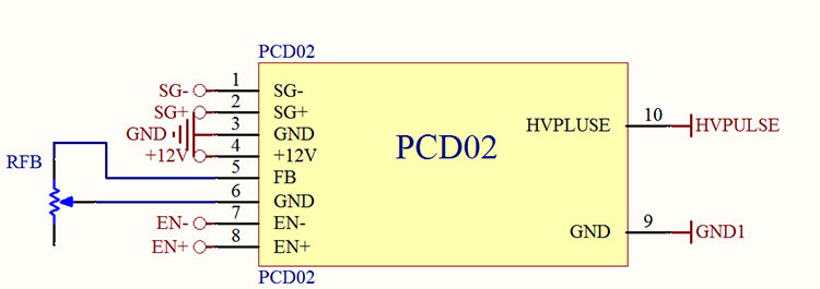
ELECTRIC BLOCK-DIAGRAM
Typical output:
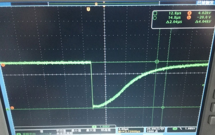
Oscillogram ofPCD02 driver operation
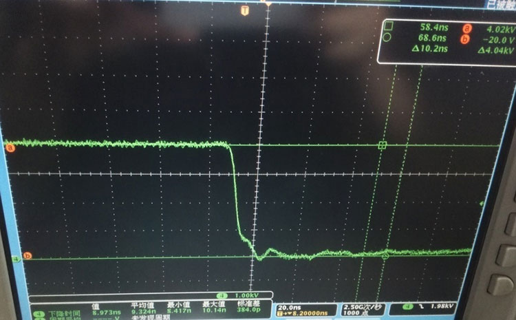
Fast edge of HV pulse in detail(fall time:8.9ns@4000V)
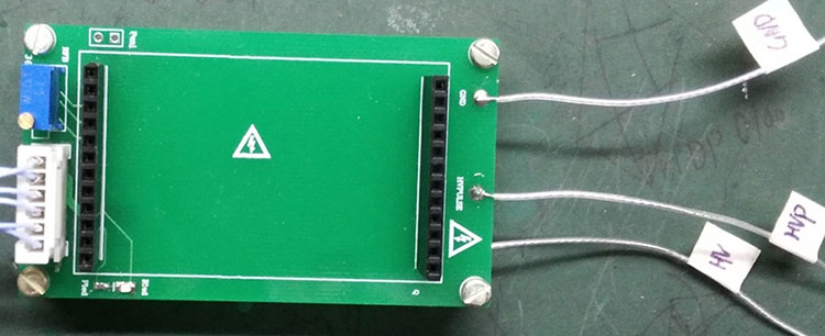
Demo Board of PCD02:
Hot Tags: Q-Switch Pockels Cell Driver, China, Wholesale, Buy, Customized, Bulk, Buy Discount, Competitive, Reliable, Good Quality, Stable Quality, Cost-effective, Advanced, Newest, Latest Selling, High Power, Regular, Stable, Reliable, Manufacturers, Suppliers, Factory, Price, Price List, Quotation, ISO9001, 1 year Warranty, Technical Support, Solution design, Scheme design
Related Category
Send Inquiry
Please feel free to give your inquiry in the form below. We will reply you in 24 hours.